
What is more valuable than gold, platinum and bitcoin? Time. Time is fleeting and once gone can never be recovered. Here at NanoES we understand this, and have developed a business model to save our customers time – and also a lot of hair pulling.
By developing and managing a network of suppliers, we are quickly able to arrange work to be done, matching the right project to the right supplier. But with a single point of contact – Nano.
It maybe prototypes are produced at one place and production elsewhere, with another supplier providing design support – but all under the Nano banner. No more time is needed to chase down and manage these suppliers – Nano has you covered.
NanoES Benefits
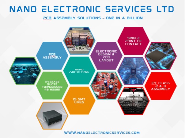
• Single point of contact
• 15 SMT lines
• Solder Jet Printing & Vapour Phase Reflow
• 3D AOI & XRAY
• uBGA, 0201 and 01005 capability
• PTH with auto insert capability
• Low cost hand build options for low volume , one off prototyping.
• IPC Class 2 & 3
• ISO13485
• Design services, including PCB layout ( Altium / Mentor ) and full product design
• Test services – EMC / environmental and vibration
• CE to UKCA support
• Rapid prototyping to box build, plus in-house design and PCB layout capabilities
• Flexible supply chain, minimising capacity issues
• Sensible quote turnaround times – typically 24-48 hours.
Why not contact NanoES to see how we can save you time – and ideally money as well.
Visit www.nanoelectronicservices.com to find out more.